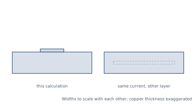
Drawn for the default inputs. It redraws as you change them.
Results are estimates. They do not replace the governing code, class or flag requirements, or a check by a competent person. Report a problem
Introduction
How wide must a PCB trace be for a given current? The trace heats up as current flows, and the width sets how much. IPC-2221 gives charts of current against copper cross-section for a chosen temperature rise. On an outer layer of 1 oz copper, 1 A with a 10 °C rise needs a trace about 12 mil (0.30 mm) wide.
This calculator applies the curve fit of the IPC-2221 charts to give the minimum trace width for your current, copper weight, temperature rise and layer. It also gives the trace's resistance, voltage drop and power loss over its length. It is for electronics designers, students and hobbyists laying out power and signal traces.
Formulas
IPC-2221 curve fit, solved for the copper cross-section:
I = k × ΔT^0.44 × A^0.725
A = (I / (k × ΔT^0.44))^(1/0.725)
w = A / t,   t = 1.378 mil × copper weight in oz/ft²
Resistance, voltage drop and loss of the trace:
R = ρ20 × (1 + α (T − 20)) × L / (w × t)
V = I × R,   P = I² × R
I — current, A; ΔT — temperature rise above ambient, °C
A — copper cross-section, mil² (1 mil = 0.001 in = 25.4 µm)
k — 0.048 for outer layers, 0.024 for inner layers
w — trace width; t — copper thickness; L — trace length
ρ20 = 1.7241 × 10⁻⁸ Ω·m, α = 0.00393 per °C; T — ambient plus rise
Assumptions and limitations
The fit is only used inside the IPC-2221 charts: up to 35 A on outer and 17.5 A on inner layers, widths up to 400 mil, rises of 10 to 100 °C, and 0.5 to 3 oz copper. Outside that range the calculator gives an error.
IPC-2221 is conservative. The newer IPC-2152 allows for the board material, its thickness and nearby copper planes. It usually permits narrower traces, especially on inner layers.
Inner layers get half the current of outer layers in IPC-2221, because the surrounding laminate traps the heat.
One ounce of copper is taken as 35 µm thick. Plating adds copper on outer layers and etching removes some, so the real section differs.
Several hot traces close together, or a trace over a heat source, run hotter than a single trace.
Worked example
A 2 A supply trace on an outer layer of 1 oz copper may rise 10 °C above an ambient of 25 °C. It is 2 in long. How wide must it be, and what does it lose?
Voltage drop: 2 × 0.0339 = 67.8 mV, and power loss: 2² × 0.0339 = 0.136 W.
The same current on an inner layer needs 80.0 mil, about 2.6 times as wide.
The worked example, drawn by the same code as the live drawing above.
FAQ
How wide should a PCB trace be for 1 A?
About 12 mil (0.30 mm) on an outer layer of 1 oz copper for a 10 °C rise. Allowing a 20 °C rise brings it down to about 8 mil.
How wide should a trace be for 3 A or 5 A?
On 1 oz outer copper with a 10 °C rise, 3 A needs about 54 mil (1.37 mm) and 5 A about 109 mil (2.77 mm).
Does 2 oz copper halve the trace width?
Yes, for the same current and rise. The cross-section stays the same, so twice the thickness needs half the width.
Why do inner layers need wider traces?
The laminate around them holds the heat in. IPC-2221 gives them half the current of an outer trace with the same section, so they need about 2.6 times the width.
What temperature rise should I allow?
10 °C is a common, cautious choice. 20 to 30 °C is often accepted for power traces, provided the board stays well below the laminate's temperature limit.
Should I use IPC-2221 or IPC-2152?
IPC-2152 is based on newer and wider measurements and gives more accurate results. IPC-2221 errs on the safe side, so a trace sized by it is rarely too narrow.
Before every release the calculator must reproduce each case below. The note under each case says where the expected answer comes from: a standard, a textbook, a published table, or a hand calculation shown in full.
1 A, 1 oz, 10 °C rise, outer layer: 16.3 mil² and 11.8 mil (0.30 mm), the value printed in IPC-2221 trace-width tablesIPC-2221B Figure 6-4 curve fit, I = 0.048 ΔT^0.44 A^0.725; 1 oz = 1.378 mil
The fitted current from the computed area returns the input current (inverse of I = k ΔT^0.44 A^0.725)IPC-2221B curve fit, hand inversion
Inner layer at 1 A needs the same copper as an outer layer at 2 A (k = 0.024 is half of 0.048)IPC-2221B: the internal chart is the external chart at half the current
2 A worked example: 2 in at 35 °C is 33.9 mΩ (R = ρ L / A with ρ = 1.7241e-8 × (1 + 0.00393 × 15)), 67.8 mV, 0.136 WIEC 60028 copper resistivity and temperature coefficient; hand calculation
Outside the IPC-2221 charts the calculator refuses: 20 A on an inner layer, a width over 400 mil, a 5 °C rise, 4 oz copperIPC-2221B chart extent (35 A outer, 17.5 A inner, 400 mil, 10–100 °C, 0.5–3 oz)
Worked example of the article: the calculator reproduces 42.4, 30.8 mil, 0.781 mm, 33.9 mΩ, 67.8 mV, 0.136 W to the digits printedThe worked example on this page, to the digits printed
Assumptions and sources
Assumptions and limits
The width comes from the curve fit to the IPC-2221 current charts, I = k ΔT^0.44 A^0.725, with k = 0.048 for outer layers and 0.024 for inner layers; the inner-layer chart is the outer one at half the current.
The fit is used only within the charts it was drawn from: currents up to 35 A on outer and 17.5 A on inner layers, widths up to 400 mil (10.2 mm), temperature rises of 10 to 100 °C and copper of 0.5 to 3 oz/ft²; outside that range the calculator refuses rather than extrapolates.
IPC-2221 is conservative. IPC-2152 (2009) is based on newer measurements and takes the board material, thickness and copper planes into account; it usually allows narrower traces, especially on inner layers.
Copper thickness is the nominal 1.378 mil (35 µm) per oz/ft²; plating on outer layers adds thickness and etching removes some, so the real cross-section differs.
Resistance uses annealed copper, 1.7241 × 10⁻⁸ Ω·m at 20 °C with 0.393 % per K, at the ambient temperature plus the temperature rise; electrodeposited PCB copper is a few per cent more resistive.
Sources
IPC-2221B, Generic Standard on Printed Board Design (2012), §6.2 Conductive material requirements and Figure 6-4, conductor current-carrying capacity charts for internal and external conductors
IPC-2152, Standard for Determining Current Carrying Capacity in Printed Board Design (2009), named for comparison
IEC 60028:1925 International standard of resistance for copper (1/58 Ω·mm²/m at 20 °C, 0.00393 per K)